- 您现在的位置:买卖IC网 > Sheet目录2005 > LTC2262CUJ-14#TRPBF (Linear Technology)IC ADC 14BIT 150MSPS 40-QFN
LTC2262-14
14
226214fc
For more information www.linear.com/LTC2262-14
CONVERTER OPERATION
The LTC2262-14 is a low power 14-bit 150Msps A/D
converter that is powered by a single 1.8V supply. The
analog inputs should be driven differentially. The encode
input can be driven differentially, or single ended for lower
power consumption. The digital outputs can be CMOS,
double data rate CMOS (to halve the number of output
lines), or double data rate LVDS (to reduce digital noise in
the system.) Many additional features can be chosen by
programming the mode control registers through a serial
SPI port. See the Serial Programming Mode section.
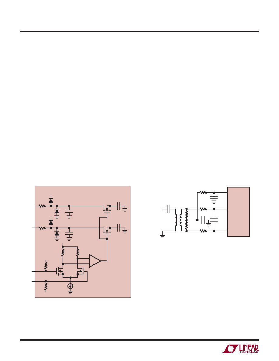
ANALOG INPUT
The analog input is a differential CMOS sample-and-hold
circuit(Figure2).Theinputsshouldbedrivendifferentially
around a common mode voltage set by the VCM output
pin, which is nominally VDD/2. For the 2V input range, the
inputs should swing from VCM– 0.5V to VCM + 0.5V. There
should be 180° phase difference between the inputs.
INPUT DRIVE CIRCUITS
Input filtering
If possible, there should be an RC lowpass filter right at
the analog inputs. This lowpass filter isolates the drive
circuitry from the A/D sample-and-hold switching, and
alsolimitswidebandnoisefromthedrivecircuitry.Figure 3
shows an example of an input RC filter. The RC component
values should be chosen based on the application’s input
frequency.
Transformer Coupled Circuits
Figure 3 shows the analog input being driven by an RF
transformer with a center-tapped secondary. The center
tap is biased with VCM, setting the A/D input at its optimal
CSAMPLE
3.5pF
RON
25
RON
25
VDD
LTC2262-14
AIN+
226214 F02
CSAMPLE
3.5pF
VDD
AIN–
ENC–
ENC+
1.2V
10k
1.2V
10k
CPARASITIC
1.8pF
CPARASITIC
1.8pF
10
25
50
0.1F
AIN+
AIN–
12pF
0.1F
VCM
LTC2262-14
ANALOG
INPUT
0.1F
T1
1:1
T1: MA/COM MABAES0060
RESISTORS, CAPACITORS
ARE 0402 PACKAGE SIZE
226214 F03
Figure 2. Equivalent Input Circuit
Figure 3. Analog Input Circuit Using a Transformer.
Recommended for Input Frequencies from 5MHz to 70MHz
APPLICATIONS INFORMATION
发布紧急采购,3分钟左右您将得到回复。
相关PDF资料
LTC2262IUJ-12#PBF
IC ADC 12BIT 150MSPS 40-QFN
LTC2264CUJ-12#PBF
IC ADC 12BIT SER/PAR 40M 40-QFN
LTC2268IUJ-14#TRPBF
IC ADC 14BIT 125MSPS DUAL 40QFN
LTC2280CUP#PBF
IC ADC DUAL 10BIT 105MSPS 64-QFN
LTC2281IUP#PBF
IC ADC 10BIT DUAL 64-QFN
LTC2282CUP#PBF
IC ADC DUAL 12BIT 105MSPS 64-QFN
LTC2284CUP#PBF
IC ADC DUAL 14BIT 105MSPS 64-QFN
LTC2285CUP#PBF
IC ADC DUAL 14BIT 125MSPS 64QFN
相关代理商/技术参数
LTC2262IUJ-12#PBF
功能描述:IC ADC 12BIT 150MSPS 40-QFN RoHS:是 类别:集成电路 (IC) >> 数据采集 - 模数转换器 系列:- 标准包装:1 系列:- 位数:14 采样率(每秒):83k 数据接口:串行,并联 转换器数目:1 功率耗散(最大):95mW 电压电源:双 ± 工作温度:0°C ~ 70°C 安装类型:通孔 封装/外壳:28-DIP(0.600",15.24mm) 供应商设备封装:28-PDIP 包装:管件 输入数目和类型:1 个单端,双极
LTC2262IUJ-12#TRPBF
功能描述:IC ADC 12BIT 150MSPS 40-QFN RoHS:是 类别:集成电路 (IC) >> 数据采集 - 模数转换器 系列:- 标准包装:1 系列:- 位数:14 采样率(每秒):83k 数据接口:串行,并联 转换器数目:1 功率耗散(最大):95mW 电压电源:双 ± 工作温度:0°C ~ 70°C 安装类型:通孔 封装/外壳:28-DIP(0.600",15.24mm) 供应商设备封装:28-PDIP 包装:管件 输入数目和类型:1 个单端,双极
LTC2262IUJ-14#PBF
制造商:Linear Technology 功能描述:ADC Single Pipelined 150Msps 14-bit Parallel/LVDS 40-Pin QFN EP 制造商:Linear Technology 功能描述:IC ADC 14BIT 1.8V 150MSPS 40-QFN
LTC2262IUJ-14#TRPBF
制造商:Linear Technology 功能描述:ADC Single Pipelined 150Msps 14-bit Parallel/LVDS 40-Pin QFN EP T/R 制造商:Linear Technology 功能描述:IC ADC 14BIT 150MSPS 40-QFN
LTC2263-12
制造商:LINER 制造商全称:Linear Technology 功能描述:12-Bit, 65Msps/40Msps/25Msps Low Power Dual ADCs
LTC2263-14
制造商:LINER 制造商全称:Linear Technology 功能描述:Quad 14-Bit, 125Msps ADC with Integrated Drivers
LTC2263CUJ-12#PBF
功能描述:IC ADC 12BIT SER/PAR 25M 40-QFN RoHS:是 类别:集成电路 (IC) >> 数据采集 - 模数转换器 系列:- 标准包装:1 系列:microPOWER™ 位数:8 采样率(每秒):1M 数据接口:串行,SPI? 转换器数目:1 功率耗散(最大):- 电压电源:模拟和数字 工作温度:-40°C ~ 125°C 安装类型:表面贴装 封装/外壳:24-VFQFN 裸露焊盘 供应商设备封装:24-VQFN 裸露焊盘(4x4) 包装:Digi-Reel® 输入数目和类型:8 个单端,单极 产品目录页面:892 (CN2011-ZH PDF) 其它名称:296-25851-6
LTC2263CUJ-12#PBF
制造商:Linear Technology 功能描述:IC ADC 12BIT 25MSPS QFN-40